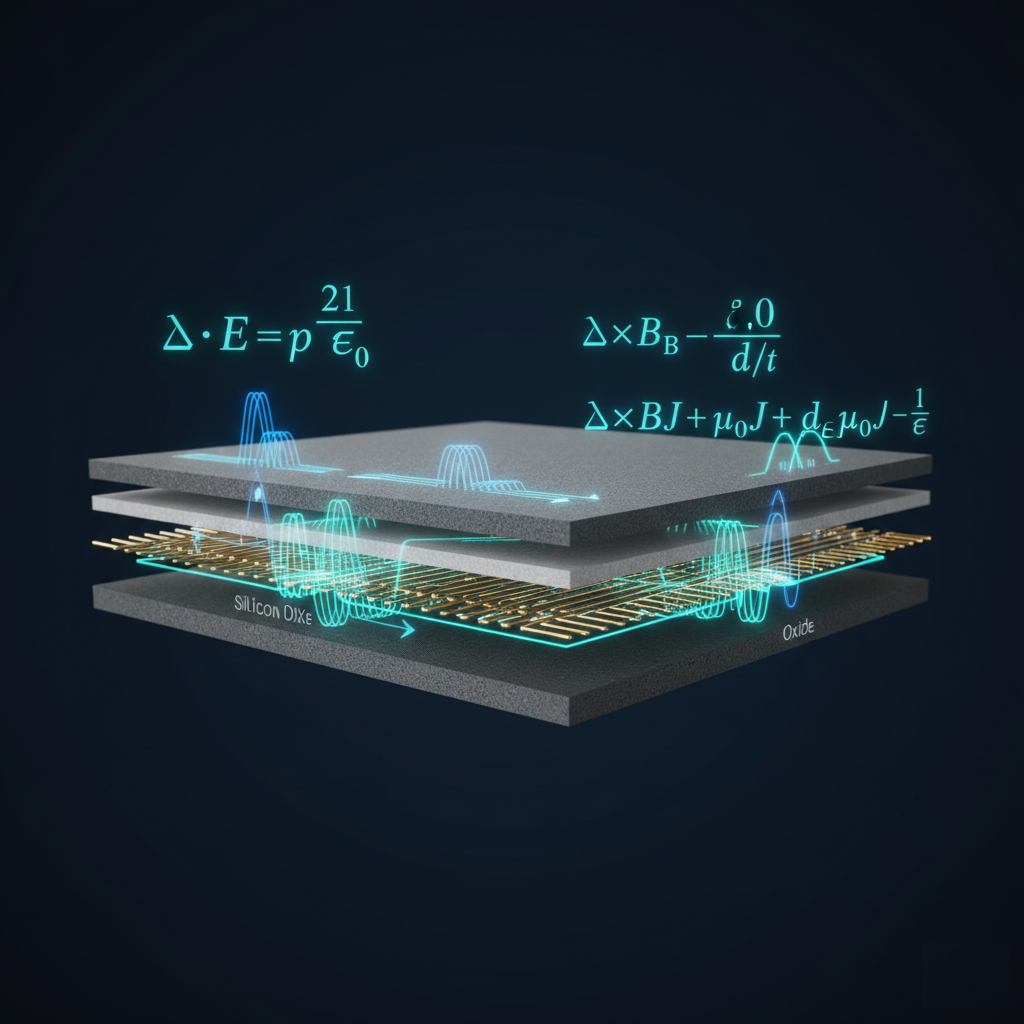
Accelerating Materials Innovation.

With focus on Semiconductor Industry.

Material development for Semiconductor Industry for Logic, Power, Photonics, Quantum. SemiCopilot brings AI-native intelligence to SiC and GaN fabs - compressing yield cycles, accelerating materials discovery, and putting Europe at the frontier of next-generation power semiconductor production.

Who we are

Challenges

SemiCopilot is solving the challenges of Long Cycles of New Material Development and corresponding Yield Losses.

The world’s transition to clean energy, electric mobility, and advanced defense electronics runs on material development. Silicon carbide and gallium nitride are no longer emerging materials - they are the backbone of the next industrial era. Yet the fabs producing them still depend on manual process expertise, fragmented toolchains, and slow empirical iteration. Every yield loss is measured in hundreds of thousands of euros. Every delayed qualification is a missed market window.

Building AI based physics simulation software for semiconductor manufacturing.

Headquartered in Germany and embedded in Europe.

Industry Verticals

Advanced Material Applications in Semiconductor Industry

Logic / Memory

Silicon (Si)

Power / RF

SiC / GaN / GaAs

Photonics

SiPh / InP / LiNbO3

Quantum

Diamond / Sapphire

Why Semi Copilot

Trusted AI agents for Semiconductor physics simulations

Our AI based Semiconductor physics simulation software utilizes existing fab data, connecting not only physics simulated data but also process parameters, equipment states, and wafer metrology, to predict and prevent yield loss before it occurs. No new hardware. No operational disruption. Pure software intelligence layered onto what fabs already have.

Accelerated Material discovery through AI

Qualifying a new material (SiC, GaN, LiNb03, Diamond, Sapphire) variant through conventional experimentation takes years. Our AI guided discovery platform replaces trial-and-error cycles with predictive screening, cutting qualification timelines from years to months and dramatically reducing R&D cost per innovation cycle.

European Sovereignty by Design

SemiCopilot is purpose-built for the European compound semiconductor ecosystem. CRMA-aligned, GDPR-compliant, and anchored in EU regulatory frameworks. Our platform supports EU Chips Act industrial goals and integrates with European pilot line and RTO infrastructure. Data stays within European borders - by architecture, not just by policy.

Technology

The Semiconductor AI Platform

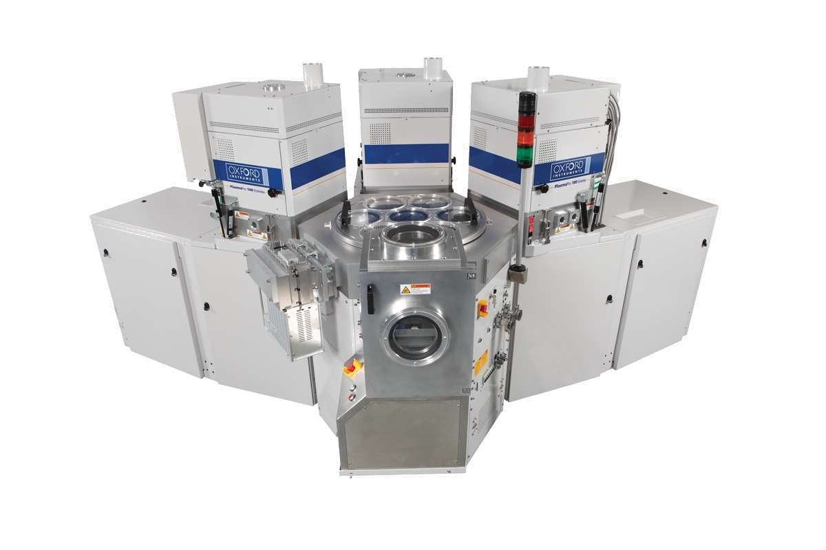
Plasma Etching AI

Plasma Etching AI

Semi Copilot provides physics-informed AI models for plasma behavior and surface evolution in semiconductor etching processes. Plasma models take inputs such as precursor gases (SF₆, C₄F₈, Cl₂, BCl₃, C₄F₈+O₂), power configurations (ICP, CCP), pressure, and chamber geometry, and predict key outputs including Ion Energy Distribution Functions (IEDF), ion flux, and electron density profiles. These outputs are tightly coupled with surface topography models that simulate material-specific etch behavior across Si, SiO₂, SiC, and GaN. The platform captures critical KPIs such as etch rate, anisotropy, selectivity, and CD bias. By combining AI with DFT/MD-informed surface kinetics, it enables predictive control of etch profiles and defect mechanisms across complex multi-step recipes.

MOCVD AI

MOCVD AI

Our AI models for MOCVD growth processes, specifically tuned for compound semiconductors such as GaN. The models take precursor inputs such as TMGa, NH₃, and dopant sources like ferrocene (Fe), SiH₄, or Cp₂Mg, along with reactor conditions including temperature, pressure, and flow dynamics. The system predicts growth rates, doping concentrations, and impurity incorporation profiles across the wafer. It further models interface quality KPIs such as dislocation density, surface roughness, and buffer layer resistivity. These insights enable optimization of GaN buffer layers, HEMT structures, and hetero-interfaces for high-performance RF and power devices.

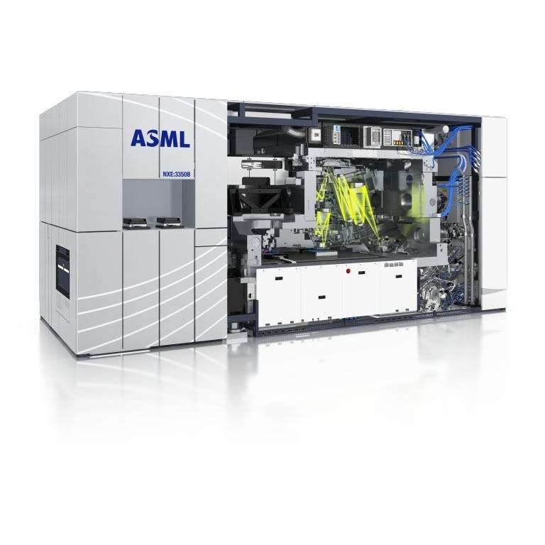
Photolithography AI

Photolithography AI

Semi Copilot enables AI-driven modeling of photolithography processes for advanced logic and emerging 2D semiconductor materials. The models take inputs such as photoresist chemistry, exposure dose, wavelength, and etch compatibility constraints to predict pattern fidelity and defect formation. Special focus is given to chemical incompatibilities and damage mechanisms in sensitive materials like MoS₂ and other 2D layers. The system identifies risks such as resist residue interaction, plasma-induced damage, and line-edge roughness. This allows engineers to co-optimize lithography and downstream processes for defect-free pattern transfer in next-generation device architectures.

Partner 1
Partner 2
Partner 3
Partner 4
Partner 5
Partner 6

Products

Material development sit at the core of electrification, clean energy, and sovereign defense electronics. SemiCopilot’s two product lines address the full production intelligence stack - from materials design to fab- floor yield.

MaterialsAI
AI-Accelerated Materials Discovery for Fabs

MaterialsAI

AI Recipe Simulator

Getting a new material (SiC, GaN, Diamond, Sapphire etc) variant from lab synthesis to production-qualified status can take three to five years of iterative physical experimentation. Semi Copilot simulates the Electrical, Topography, Optical, Thermal and Mechchanical properties instantly through the power of our pretrained AI algorithms for a given material and a given device geometry, and accordingly gives the most optimal recipe to run inside the Fab.

Explore MaterialsAI
FabverseAI
AI-Powered Yield Optimization for Fabs

FabverseAI

Tool Drift Forecaster

Advanced-age semiconductor fabs operate at the edge of process complexity. A single defect cluster in SiC epitaxy, an uncontrolled doping gradient, or a mistimed anneal step can cascade into wafer-level yield loss worth hundreds of thousands of euros per run. As opposed to the industry’s current response (manual engineering intuition and reactive process corrections), Semi Copilot gives you a very accurate and reliable Process/Equipment Development.

Request a FabverseAI Demo

Our Leadership Team

Pradeep Tripathi

Pradeep Tripathi

Co-Founder (Revenue)

NTU Taiwan

Rahul Prajapat

Rahul Prajapat

Co-Founder (Product)

IIT Bombay • Serial Entrepreneur

Prof. Abhishek Singh

Prof. Abhishek Singh

Co-Founder (Science)

UC Santa Barbara

Dr. Stefan F. Müller

Dr. Stefan F. Müller

Advisor

TU Dresden • TU Munich

Connect US

Visit Semi Copilot Europe

Connecting with the heart of European semiconductor innovation. Reach out to us directly or visit one of our offices.

Dresden

Headquarters

Friedlandstraße 5, 01445
Radebeul,
Germany


Get Directions

Munich

Branch

Zugspitz Str. 80A, Gauting
82131, Bayern,
Germany


Get Directions